The future of technology is here, and it’s being shaped by advanced innovations that are pushing the boundaries of what we thought was possible. In the semiconductor industry, three groundbreaking chips have emerged, revolutionizing the fields of AI, computing, and beyond. NVIDIA’s Blackwell GPU, Cerebras wafer-scale engine chip, and the EnCharge analog chip are ushering in a new era of performance, efficiency, and breakthroughs.
These advanced chips are not just incremental improvements; they are redefining the very fabric of our technological landscape. With their exceptional capabilities and innovative designs, they are opening up new possibilities in fields such as natural language processing, computer vision, and energy efficiency. The future is brighter than ever, thanks to these game-changing advancements.
Table of Contents
Key Takeaways:
- Three groundbreaking chips – NVIDIA’s Blackwell GPU, Cerebras wafer-scale engine chip, and the EnCharge analog chip – are redefining what’s possible in tech.
- These advanced chips are revolutionizing AI, computing, and other industries, pushing the boundaries of performance and efficiency.
- They are opening up new possibilities in natural language processing, computer vision, and energy efficiency.
- The future is brighter than ever, thanks to these game-changing advancements.
- Stakeholders need to engage in meaningful discussions and collaborations to ensure responsible and equitable use of these advanced innovations.
NVIDIA’s Blackwell GPU: Revolutionizing Performance in AI
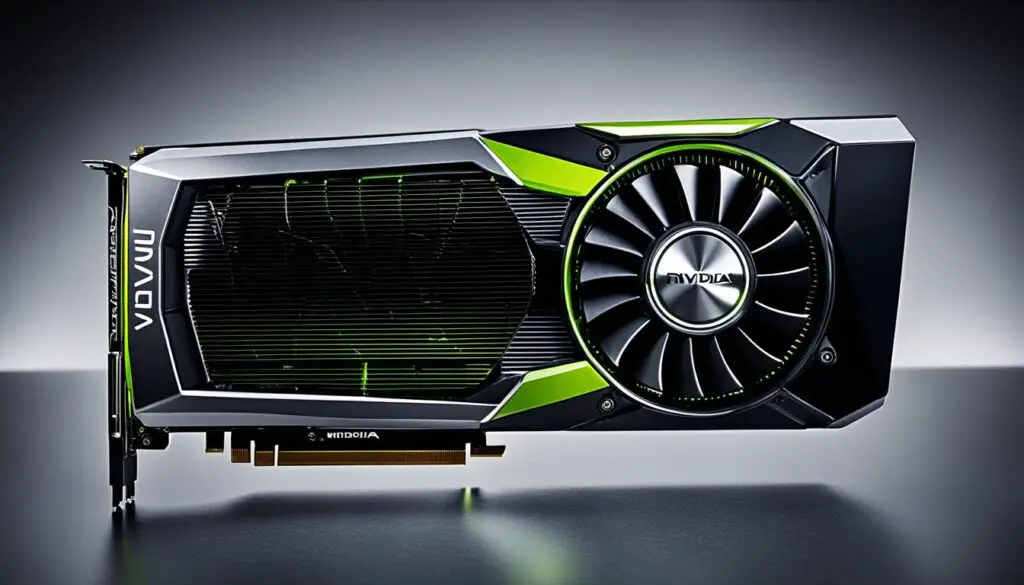
NVIDIA, a leader in AI hardware, has taken performance to new heights with its revolutionary Blackwell GPU. This cutting-edge technology is reshaping the AI landscape and pushing the boundaries of what is possible.
With an astonishing 208 billion transistors, the Blackwell GPU delivers unmatched power and efficiency. Its capabilities are truly groundbreaking, offering quadruple the training performance and a remarkable 30-fold increase in inference performance compared to its predecessors. This outstanding level of performance enables faster and more accurate AI computations, propelling advancements in various fields.
The Blackwell GPU’s innovative dual-die design and advanced packaging technology contribute to its exceptional performance. By maximizing interconnect density and bandwidth, NVIDIA has created a GPU that is tailor-made for demanding AI applications. Whether it’s natural language processing, computer vision, or autonomous systems, the Blackwell GPU delivers remarkable results, driving forward breakthroughs in AI.
“With its unparalleled performance, NVIDIA’s Blackwell GPU is a game-changer in the AI hardware sector. Its remarkable capabilities in natural language processing, computer vision, and autonomous systems have the potential to revolutionize industries and drive innovation to new heights.”
Key Features and Benefits of the Blackwell GPU
The Blackwell GPU offers a host of features and benefits that make it stand out in the world of AI hardware. Here are some key highlights:
- Unprecedented performance with 208 billion transistors
- Quadruple the training performance compared to previous GPUs
- 30-fold increase in inference performance
- Dual-die design for high interconnect density
- Advanced packaging technology for enhanced bandwidth
These features enable the Blackwell GPU to handle even the most complex AI tasks with ease, opening up new possibilities for AI-driven solutions.

Comparative Performance of NVIDIA GPUs
| GPU Model | Transistor Count | Training Performance (Quadruple Improvement) | Inference Performance (30-fold Increase) |
|---|---|---|---|
| Blackwell GPU | 208 billion | ✓ | ✓ |
| Previous Generation GPU | Varies | ✗ | ✗ |
As the comparison table above illustrates, the Blackwell GPU outperforms previous generation GPUs across the board, highlighting its exceptional performance and breakthrough capabilities.
The Blackwell GPU from NVIDIA is revolutionizing performance in AI, pushing the boundaries of what is possible. With its unrivaled processing power and efficiency, it is driving breakthroughs in various AI applications and paving the way for a future powered by intelligent systems.
Cerebras Wafer-Scale Engine Chip: Handling Massive AI Models with Ease
The Cerebras wafer-scale engine chip is a revolutionary breakthrough in AI technology, designed to handle massive AI models with unparalleled efficiency. With its impressive 4 trillion transistors and monolithic design, this chip is pushing the boundaries of what is possible in AI computation.

Manufactured using cutting-edge 5nm process technology, the Cerebras wafer-scale engine chip offers significant advantages in handling AI models and datasets. It eliminates the complexities associated with interconnecting multiple GPUs, simplifying AI tasks and improving overall performance.
This chip’s efficiency in handling massive AI models has transformative implications across various fields. In scientific research, the Cerebras chip enables faster analysis and processing of complex data, accelerating breakthroughs in fields such as genomics and drug discovery. The chip’s computational power also has vast potential in climate modeling, enhancing our understanding of climate change and informing sustainable solutions.
Furthermore, the wafer-scale design of the Cerebras chip presents new possibilities for training and deploying large-scale AI systems. Its extensive interconnectivity and high-speed data transfer capabilities revolutionize the way we approach AI applications, enabling faster model training and deployment for real-world use cases.
“The Cerebras wafer-scale engine chip represents a monumental leap forward in AI computing. Its ability to handle massive AI models with ease opens up new opportunities for scientific discovery, precision medicine, and climate research.”
In summary, the Cerebras wafer-scale engine chip is a game-changer in AI technology, with its unprecedented performance and efficiency. It empowers researchers, scientists, and organizations to tackle complex AI tasks with ease, leading to groundbreaking advancements across various industries.
| Advantages of the Cerebras Wafer-Scale Engine Chip: |
|---|
| Unmatched performance and efficiency |
| Simplified AI tasks by eliminating complexities |
| Ability to handle massive AI models and datasets |
| Faster analysis and processing of complex data |
| Revolutionizes AI model training and deployment |
EnCharge Analog Chip: Energy-Efficient Computing for the Future
The EnCharge analog chip revolutionizes computing with its groundbreaking approach to energy-efficient processing. By employing near-memory or in-memory computing using charge-domain computation, this chip achieves a remarkable 20x improvement in energy efficiency compared to its predecessors. This significant advancement directly addresses the persistent memory bottleneck challenge that has long constrained computing tasks.
One of the key advantages of the EnCharge analog chip is its ability to minimize data movement, resulting in substantial energy savings and improved performance. By performing computations closer to the memory, the EnCharge chip reduces the need for data to be transferred between the processor and memory, thus optimizing power consumption. This breakthrough technology enables devices to operate for longer periods on a single charge and enhances overall system efficiency.
The EnCharge analog chip finds extensive applications in cutting-edge fields such as edge computing, IoT devices, and battery-powered applications. In the context of edge computing, where processing tasks are performed at or near the source of data generation, the EnCharge chip’s energy efficiency is particularly valuable. It allows edge devices to deliver powerful computation while minimizing power consumption, making them ideal for resource-constrained environments.
In the realm of IoT devices, characterized by their small form factors and limited power capabilities, the EnCharge analog chip brings remarkable benefits. It enables efficient processing and data storage within these devices, paving the way for more sophisticated functionalities and enhanced user experiences. Additionally, the EnCharge chip’s energy efficiency contributes to extended battery life, reducing the need for frequent recharging and bringing convenience to IoT device users.
Furthermore, the EnCharge analog chip plays a crucial role in driving energy efficiency and sustainability in the computing industry. By significantly reducing power consumption and enhancing overall efficiency, this chip aligns with the growing need for environmentally friendly computing solutions. As the world places increasing importance on energy conservation and sustainable practices, the EnCharge analog chip emerges as an essential component in shaping a greener and more efficient future.
In summary, the EnCharge analog chip represents a major leap forward in energy-efficient computing. Its utilization of charge-domain computation and near-memory processing significantly improves energy efficiency while addressing memory bottlenecks. With applications in edge computing, IoT devices, and battery-powered applications, the EnCharge chip is poised to drive the next phase of technological innovation.
Conclusion: The Future of Semiconductor Innovation
The semiconductor industry is driving remarkable innovation through the development of advanced chips like NVIDIA’s Blackwell GPU, Cerebras wafer-scale engine chip, and the EnCharge analog chip. These cutting-edge technologies are revolutionizing the possibilities in the tech world, pushing the boundaries of processing power, efficiency, and energy savings.
As these advanced chips become more widely adopted, we can anticipate a proliferation of intelligent systems and applications that will transform industries and revolutionize scientific research. The rapid pace of innovation in the semiconductor industry holds exciting potential for the future, opening up new avenues in computing and unlocking endless possibilities.
However, this rapid progress also brings forth important challenges and questions. The increasing demand for processing power and data raises concerns around energy consumption, data privacy, and ethical implications. It is vital for stakeholders in the semiconductor industry to engage in meaningful discussions and collaborations to ensure responsible and equitable use of these advanced innovations.
In conclusion, the future of computing is bright thanks to advancements in the semiconductor industry. These advanced chips are at the forefront of innovation and will shape the tech landscape for years to come. By leveraging the immense power and efficiency of technologies like NVIDIA’s Blackwell GPU, Cerebras wafer-scale engine chip, and the EnCharge analog chip, we can embrace a future filled with possibilities and transformative breakthroughs in computing.
FAQ
What are the three groundbreaking chips in the semiconductor industry?
The three groundbreaking chips in the semiconductor industry are NVIDIA’s Blackwell GPU, Cerebras wafer-scale engine chip, and the EnCharge analog chip.
What is special about NVIDIA’s Blackwell GPU?
NVIDIA’s Blackwell GPU offers unprecedented performance with its 208 billion transistors. It provides quadruple the training performance and a 30-fold increase in inference performance compared to its predecessors. Its dual-die design and advanced packaging technology enable high interconnect density and bandwidth, making it ideal for AI applications.
What is unique about Cerebras wafer-scale engine chip?
The Cerebras wafer-scale engine chip stands out with its 4 trillion transistors and monolithic design. It simplifies AI tasks by eliminating the complexities of interconnecting multiple GPUs. This chip can handle massive AI models and datasets with unprecedented speed and efficiency, making it a game-changer in scientific research, drug discovery, and climate modeling.
What is the EnCharge analog chip known for?
The EnCharge analog chip introduces a pioneering approach to computing with its near-memory or in-memory computing using charge-domain computation. It achieves at least 20 times more energy-efficiency than its analog predecessors, addressing the persistent memory bottleneck challenge in computing tasks. Its applications in edge computing, IoT devices, and battery-powered applications make it a key player in the drive for energy efficiency and sustainable computing solutions.
How are these advanced chips reshaping the technological landscape?
These advanced chips are pushing the limits of processing power and efficiency in AI and computing applications. They are reshaping the technological landscape by opening up new possibilities in fields such as natural language processing, computer vision, and energy efficiency. Their exceptional performance and innovative designs are revolutionizing the way we approach AI and computing tasks.
What can we expect in the future with the widespread adoption of these advanced chips?
With the widespread adoption of these advanced chips, we can expect to see a proliferation of intelligent systems and applications that will transform industries and revolutionize scientific research. The rapid pace of innovation in the semiconductor industry promises exciting possibilities for the future, but also raises important questions and challenges around energy consumption, data privacy, and ethical implications. It is crucial for stakeholders to engage in meaningful discussions and collaborations to ensure responsible and equitable use of these advanced innovations.


